Daily a plethora of data is being generated and the computing power to process this data into useful information is stalling. One of the fundamental problems being faced is the processor-memory bottleneck or the performance gap. Various methods such as caches and different software techniques have been used to eliminate this problem. But there’s another way which is, building the CPU directly into a 3D memory structure, connect them directly without any kind of motherboard traces, and compute from within the RAM itself.

A prototype chip built by researchers at Stanford and MIT can solve the problem by sandwiching the memory, processor and even sensors all into one unit. While current chips are made of silicon
.
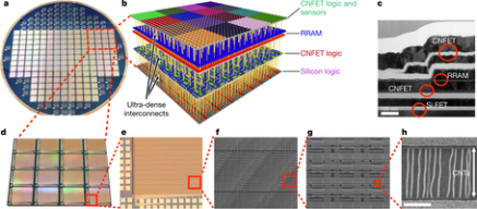
The researchers have developed a new 3D chip fabrication method that uses carbon nanotubes and resistive random-access memory (RRAM) cells together to create a combined nanoelectronic processor design that supports complex, 3D architecture – where traditional silicon-based chip fabrication works with 2D structures only. The team claims this makes for “the most complex nanoelectronic system ever made with emerging nanotechnologies,” creating a 3D computer architecture. Using carbon makes the whole thing possible since higher temperatures required to make a silicon CPU would damage the sensitive RRAM cells.
The 3D design is possible because these carbon nanotube circuits and RRAM memory components can be made using temperatures below 200 degrees Celsius, which is far, far less than the 1,000 degree temps needed to fabricate today’s 2D silicon transistors. Lower temperatures mean you can build an upper layer on top of another without damaging the one or ones below.
One expert cited by MIT said that this could be the answer to continuing the exponential scaling of computer power in keeping with Moore’s Law, as traditional chip methods start to run up against physical limits. It’s still in its initial phases and it would take many years till we see the actual implementation of these chips in real life.
 satta king gali