New Algorithm that outperforms Deep Learning

Deep Learning is blooming and with it, all kinds of unthought applications have been sprung to life. Every tech company is trying to implement a form of AI in their businesses in some way or the other. Neural networks, after all, have begun to outperform humans in tasks such as object and face recognition and in games such as chess, Go, and various arcade video games. And as we all know, Deep Learning is a manifestation of the human brain and has tremendous potential.

However, An entirely different type of computing has the potential to be significantly more powerful than neural networks and deep learning. This technique is based on the process that created the human brain—evolution. In other words, a sequence of iterative change and selection that produced the most complex and capable machines known to humankind—the eye, the wing, the brain, and so on. The power of evolution is a wonder to behold.

atari-evolutionary-comp.jpg

Evolution


Evolutionary computing is completely unlike Deep Learning. The conventional way to create code is to write it from first principles with a specific goal in mind. Evolutionary computing uses a different approach. It starts with code generated entirely at random. And not just one version of it, but lots of versions, sometimes hundreds of thousands of randomly assembled pieces of code, and each of these codes have been tested to check whether the end goal is achieved. As a result, a lot of code is generated. But just by chance, some pieces of code are a little better than others. These pieces are then reproduced in a new generation of code, which includes more copies of the better codes.

However, the next generation cannot be an identical copy of the first. Instead, it must change in some way. These changes can involve switching two terms in the code—a kind of point mutation. Or they can involve two codes that are cut in half and the halves exchanged—like sexual recombination.

Each of the new generations is then tested to see how well it works. The best pieces of code are preferentially reproduced in another generation, and so on. In this way, the code evolves. Over time, it becomes better, and after many generations, if conditions are right, it can become better than any human coder can design.


via: MitTechReview, Medium

What is Ethereum?

With all the hype going around Blockchain and it’s infrastructure users like Bitcoin and Ethereum are all over the media and magazines I had to write a blog on Ethereum. Briefly, Blockchain is to Bitcoin, what the internet is to email. A big electronic system, on top of which you can build applications.

Then what’s Ethereum? It is a public database that keeps a permanent record of digital transactions. Importantly, this database doesn’t require any central authority to maintain and secure it.

Ethereum_large-1.png

Like Bitcoin, Ethereum is a distributed public blockchain network. Although there are some significant technical differences between the two, the most important distinction to note is that Bitcoin and Ethereum differ substantially in purpose and capability. Bitcoin offers one particular application of blockchain technology, a peer to peer electronic cash system that enables online Bitcoin payments. While the Bitcoin blockchain is used to track ownership of digital currency (bitcoins), the Ethereum blockchain focuses on running the programming code of any decentralized application.

In the Ethereum blockchain, instead of mining for bitcoin, miners work to earn Ether, a type of crypto token that fuels the network. Beyond a tradeable cryptocurrency, Ether is also used by application developers to pay for transaction fees and services on the Ethereum network.

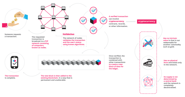
The Ethereum blockchain is essentially a transaction-based state machine, which means that on a series of specific inputs, it will transition to a new state. The first state in Ethereum is the genesis state, which means a blank state, wherein no transactions have happened on the network. After a transaction occurs, the genesis state transitions to a new state, possibly a final state denoting the current state of Ethereum. Of course, there are millions of transactions occurring concurrently, whereby these transactions are grouped in Blocks. So to simplify, a Block contains a series of transactions.

To cause a transition from one state to the next, a transaction must be valid. For a transaction to be considered valid, it must go through a validation process known as miningMining is when a group of nodes (i.e. computers) expend their compute resources to create a block of valid transactions. In the most basic sense, a transaction is a cryptographically signed piece of instruction that is generated by an externally owned account, serialized, and then submitted to the blockchain.

Any node on the network that declares itself as a miner can attempt to create and validate a block. Lots of miners from around the world try to create and validate blocks at the same time. Each miner provides a mathematical “proof” when submitting a block to the blockchain, and this proof acts as a guarantee: if the proof exists, the block must be valid.

For a block to be added to the main blockchain, the miner must prove it faster than any other competitor miner. The process of validating each block by having a miner provide a mathematical proof is known as a “proof of work.”

A miner who validates a new block is rewarded with a certain amount of value for doing this work. What is that value? The Ethereum blockchain uses an intrinsic digital token called “Ether.” The value token of the Ethereum blockchain is called ether. It is listed under the code ETH and traded on cryptocurrency exchanges. It is also used to pay for transaction fees and computational services on the Ethereum network. Every time a miner proves a block, new Ether tokens are generated and awarded. Ether can be transferred between accounts and used to compensate participant nodes for computations performed.

EVM – Ehtereum Virtual Machine

Ethereum is a programmable blockchain. Rather than give users a set of pre-defined operations (e.g. bitcoin transactions), Ethereum allows users to create their own operations of any complexity they wish. In this way, it serves as a platform for many different types of decentralized blockchain applications, including but not limited to cryptocurrencies.

Ethereum in the narrow sense refers to a suite of protocols that define a platform for decentralized applications. At the heart of it is the Ethereum Virtual Machine (“EVM”), which can execute code of arbitrary algorithmic complexity. In computer science terms, Ethereum is “Turing complete”. Developers can create applications that run on the EVM using friendly programming languages modeled on existing languages like JavaScript and Python.

Smart Contracts

Smart contracts are deterministic exchange mechanisms controlled by digital means that can carry out the direct transaction of value between untrusted agents. They can be used to facilitate, verify, and enforce the negotiation or performance of economically-laden procedural instructions and potentially circumvent censorship, collusion, and counter-party risk. In Ethereum, smart contracts are treated as autonomous scripts or stateful decentralized applications that are stored in the Ethereum blockchain for later execution by the EVM. Instructions embedded in Ethereum contracts are paid for in ether (or more technically “gas”) and can be implemented in a variety of Turing complete scripting languages.

There’s still a lot more to Ethereum, but this blog will help you get some insights before delving in deeper in the utopian world of blockchain and cryptocurrency.


(sources: Wiki, Telegraph, Medium, ethdocs)

NVIDIA’S CHIPS FOR COMPLETE CONTROL OF DRIVERLESS CARS

The race for autonomy in cars is ubiquitous. Top car brands are working in providing complete autonomous vehicles to their customers and the future with self-driving vehicles is inevitable. Adding the cherry to the cake, Nvidia’s recently announced chip is the latest generation of its DrivePX onboard car computers called Pegasus. The device is 13 times faster than the previous iteration, which has so far been used by the likes of Audi, Tesla, and Volvo to provide semi-autonomous driving capabilities in their vehicles.

nvidia_pegasus

Nvidia Pegasus

At the heart of this semiconductor is the mind-boggling technology of Deep Learning. “In the old world, the more powerful your engine, the smoother your ride will be,” Huang said during the announcement. “In the future, the more computational performance you have, the smoother your ride will be.”

Nvidia asserts that the device is only about the size of a license plate. But it has enough power to process data from up to 16 sensors, detect objects, find the car’s place in the world, plan a path, and control the vehicles itself. Oh, and it will also update centrally stored high-definition maps at the same time—all with some resources to spare.

The new system is designed to eventually handle up to 320 trillion operations per second (TOPS), compared to the 24tn of today’s technology. That would give it the power needed to process the masses of data produced by a vehicle’s cameras and other sensors and allow it to drive completely autonomously, Nvidia said. The first systems to be tested next year will have less processing power but will be designed to scale up with the addition of extra chips.


(sources: MitTechReview, NvidiaBlog)

MIT’s new prototype ‘3D’ Chip

Daily a plethora of data is being generated and the computing power to process this data into useful information is stalling. One of the fundamental problems being faced is the processor-memory bottleneck or the performance gap. Various methods such as caches and different software techniques have been used to eliminate this problem. But there’s another way which is, building the CPU directly into a 3D memory structure, connect them directly without any kind of motherboard traces, and compute from within the RAM itself.

3d.jpeg


A prototype chip built by researchers at Stanford and MIT can solve the problem by sandwiching the memory, processor and even sensors all into one unit. While current chips are made of silicon

.

rram.jpg

The researchers have developed a new 3D chip fabrication method that uses carbon nanotubes and resistive random-access memory (RRAM) cells together to create a combined nanoelectronic processor design that supports complex, 3D architecture – where traditional silicon-based chip fabrication works with 2D structures only. The team claims this makes for “the most complex nanoelectronic system ever made with emerging nanotechnologies,” creating a 3D computer architecture. Using carbon makes the whole thing possible since higher temperatures required to make a silicon CPU would damage the sensitive RRAM cells.

The 3D design is possible because these carbon nanotube circuits and RRAM memory components can be made using temperatures below 200 degrees Celsius, which is far, far less than the 1,000 degree temps needed to fabricate today’s 2D silicon transistors. Lower temperatures mean you can build an upper layer on top of another without damaging the one or ones below.

One expert cited by MIT said that this could be the answer to continuing the exponential scaling of computer power in keeping with Moore’s Law, as traditional chip methods start to run up against physical limits. It’s still in its initial phases and it would take many years till we see the actual implementation of these chips in real life.

Response of an artificial iris to light like the human eye

An artificial iris manufactured from intelligent, light-controlled polymer material can react to incoming light in the same ways as the human eye. The Iris was developed by the Smart Photonic Materials research group from the TUT, and it was recently published in the Advanced Materials journal.

iris.jpg

The human iris does its job of adjusting your pupil size to meter the amount of light hitting the retina behind without you having to actively think about it. And while a camera’s aperture is designed to work the same way as a biological iris, it’s anything but automatic. Even point-and-shoots rely on complicated control mechanisms to keep your shots from becoming overexposed. But a new “artificial iris” developed at the Tampere University of Technology in Finland can autonomously adjust itself based on how bright the scene is.

Scientists from the Smart Photonic Materials research group developed the iris using a light-sensitive liquid crystal elastomer. The team also employed photoalignment techniques, which accurately position the liquid crystal molecules in a predetermined direction within a tolerance of a few picometers. This is similar to the techniques used originally in LCD TVs to improve viewing angle and contrast but has since been adopted to smartphone screens. “The artificial iris looks a little bit like a contact lens,” TUT Associate Professor Arri Priimägi said. “Its center opens and closes according to the amount of light that hits it.”

The team hopes to eventually develop this technology into an implantable biomedical device. However, before that can happen, the TUT researchers need to first improve the iris’ sensitivity so that it can adapt to smaller changes in brightness. They also need to get it to work in an aqueous environment. However, this new iris is therefore still long ways away from being ready.

What is Blockchain?

Blockchains in Bitcoin.


A blockchain is a public ledger of all Bitcoin transactions that have ever been executed. It is constantly growing as ‘completed’ blocks are added to it with a new set of recordings. The blocks are added to the blockchain in a linear, chronological order. Each node (computer connected to the Bitcoin network using a client that performs the task of validating and relaying transactions) gets a copy of the blockchain, which gets downloaded automatically upon joining the Bitcoin network. The blockchain has complete information about the addresses and their balances right from the genesis block to the most recently completed block.

Blockchain

Blockchain formation.

The blockchain is seen as the main technological innovation of Bitcoin since it stands as proof of all the transactions on the network. A block is the ‘current’ part of a blockchain which records some or all of the recent transactions, and once completed goes into the blockchain as a permanent database. Each time a block gets completed, a new block is generated. There is a countless number of such blocks in the blockchain. So are the blocks randomly placed in a blockchain? No, they are linked to each other (like a chain) in proper linear, chronological order with every block containing a hash of the previous block.

To use conventional banking as an analogy, the blockchain is like a full history of banking transactions. Bitcoin transactions are entered chronologically in a blockchain just the way bank transactions are. Blocks, meanwhile, are like individual bank statements.

Based on the Bitcoin protocol, the blockchain database is shared by all nodes participating in a system. The full copy of the blockchain has records of every Bitcoin transaction ever executed. It can thus provide insight about facts like how much value belonged a particular address at any point in the past.

In the above representation, the main chain (black) consists of the longest series of blocks from the genesis block (green) to the current block. Orphan blocks (purple) exist outside of the main chain.


infographics0517-01

Working of Bitcoin and Blockchain


 A blockchain – originally block chain– is a distributed database that is used to maintain a continuously growing list of records, called blocks. Each block contains a timestamp and a link to a previous block. A blockchain is typically managed by a peer-to-peer network collectively adhering to a protocol for validating new blocks. By design, blockchains are inherently resistant to modification of the data. Once recorded, the data in any given block cannot be altered retroactively without the alteration of all subsequent blocks and the collusion of the network. Functionally, a blockchain can serve as “an open, distributed ledger that can record transactions between two parties efficiently and in a verifiable and permanent way. The ledger itself can also be programmed to trigger transactions automatically.”

Intel Core i9

Intel recently announced a new family of processors for enthusiasts, the Core X-series, and it’s anchored by the company’s first 18-core CPU, the i9-7980XE.


Intel+Core+i9+x+series.jpg

Priced at $1,999, the 7980XE is clearly not a chip you’ll see in an average desktop. Instead, it’s more of a statement from Intel. It beats out AMD’s 16-core Threadripper CPU, which was slated to be that company’s most powerful consumer processor for 2017. And it gives Intel yet another way to satisfy the demands of power-hungry users who might want to do things like play games in 4K while broadcasting them in HD over Twitch. And, as if its massive core count wasn’t enough, the i9-7980XE is also the first Intel consumer chip that packs in over a teraflop’s worth of computing power.


inteli9.jpg


If 18 cores are overkill for you, Intel also has other Core i9 Extreme Edition chips in 10-, 12-, 14- and 16-core variants. Perhaps the best news for hardware geeks: The 10 Core i9-7900X will retail for $999, a significant discount from last year’s version.

All of the i9 chips feature base clock speeds of 3.3GHz, reaching up to 4.3GHz dual-core speeds with Turbo Boost 2.0 and 4.5GHz with Turbo Boost 3.0 a new version of Turbo Boost which Intel has upgraded. The company points out that while the additional cores on the Core X models will improve multitasking performance, the addition of technologies like Turbo Boost Max 3.0 ensures that each core is also able to achieve improved performance. (Intel claims that the Core X series reaches 10 percent faster multithread performance over the previous generation and 15 percent faster single thread.)


(via Engadget, The Verge)


A peek into NVIDIA’s self driving AI.

In a step toward making AI more accountable, Nvidia has developed a neural network for autonomous driving that highlights what it’s focusing on.

Sorta follow-up to my previous blog post: Is AI Mysterious?. Some of the most powerful machine-learning techniques available result in software that is almost completely opaque, even to the engineers that build it.

nvidia_car.jpg

We still don’t know exactly how AI works, the people at Nvidia still don’t know why the AI they built wasn’t following a single instruction given by its creators. Instead, it relied entirely on an algorithm that had taught itself to drive by watching a human do it.

It simply matches input from several video cameras to the behavior of a human driver and figures out for itself how it should drive. The only catch is that the system is so complex that it’s difficult to untangle how it actually works.

Nvidia is now working to open the black box by developing a way to visually highlight what the system is paying attention to. Explained in a recently published paper, the neural network architecture developed by Nvidia’s researchers is designed so that it can highlight the areas of a video picture that contribute most strongly to the behavior of the car’s deep neural network. Remarkably, the results show that the network is focusing on the edges of roads, lane markings, and parked cars—just the sort of things that a good human driver would want to pay attention to.

PilotNet.png

Nvidia’s Convolutional Neural Network architecture for Self-Driving AI.

“What’s revolutionary about this is that we never directly told the network to care about these things,” Urs Muller, Nvidia’s chief architect for self-driving cars, wrote in a blog post.

Fascinatingly enough, this compares a lot to human intelligence where we don’t actually know how to describe certain actions we do, but we just do them.

This certainly highlights the fact that in the near future we might start seeing AI those are just like us or even Superintelligent. I highly recommend reading the book Superintelligence: Paths, Dangers, Strategies by Nick Bostrom.

(Sources: Nvidia, MitTechReview, Nvidia Blog)

Artificial Intelligence ready ARM CPUs (DynamIQ)

ARM processors are ubiquitous and many of the tech gadgets we used are powered by them, furthermore, the company is showing off its plans for the future with DynamIQ. Aimed squarely at pushing the artificial intelligence and machine learning systems we’re expecting to see in cars, phones, gaming consoles and everything else, it’s what the company claims is an evolution on the existing “big.Little” technology.

arm.jpg

Here’s a high-level look at some of the new features, capabilities and benefits DynamIQ will bring to new Cortex-A processors later this year:

  • New dedicated processor instructions for ML and AI: Cortex-A processors designed for DynamIQ technology can be optimized to deliver up to a 50x boost in AI performance over the next 3-5 years relative to Cortex-A73-based systems today and up to 10x faster response between CPU and specialized accelerator hardware on the SoC that can unleash substantially better-combined performance.

arm-dynamiq2.jpg

  • Increased multi-core flexibility: SoC designers can scale up to eight cores in a single cluster and each core can have different performance and power characteristics. These advanced capabilities enable faster responsiveness to ML and AI applications. A redesigned memory subsystem enables both faster data access and enhance power management
  • More performance within restricted thermal budgets: Efficient and much faster switching of software tasks to match the right-sized processor for optimal performance and power is further enhanced through independent frequency control of individual processors
  • Safer autonomous systems: DynamIQ brings greater levels of responsiveness for ADAS solution and increased safety capabilities which will enable partners to build ASIL-D compliant systems for safe operation under failure conditions.


(source: ARM community, Engadget)

Razer’s Project Valerie

For those who missed out on Razer’s CES 2017 showcase, Project Valerie is an impressive gaming laptop with three 4K displays, virtually allowing for a portable panoramic display mode.

Each display is 17.3 inches in size and features a 4K resolution, offering a huge viewing space unprecedented for a laptop. When not in use, the extra Project Valerie screens are housed within a chassis. When the laptop is opened, the screens automatically slide out from the lid and extend to the sides of the main display to create a 180-degree viewing experience, without requiring any human input.

Razer-Valerie-_-featured-640x360@2x.jpg

The machine is fuelled by a top-of-the-line Nvidia GeForce GTX 1080 graphics card with 8GB RAM, accompanied by an Intel Core i7 Skylake CPU and 32GB RAM as a foundation. It seems to be all about graphics power, and since Razer has a reputation for building high-end gaming laptops, Project Valerie is certainly no exception.

Since these two extra 17″ 4K displays need some extra space, the unit is somewhat thick in comparison to the paper-thin laptops of today and is not exactly lightweight either. But for what it is, it’s pretty impressive.

For more information, watch the video linked below.