Google’s Bristlecone Quantum Computing Chip

A few days ago Google previewed its new quantum processor, Bristlecone, a quantum computing chip that will serve as a testbed for research regarding the system error rates and scalability of Google’s qubit technology. In a post on its research blog, Google said it’s “cautiously optimistic that quantum supremacy can be achieved with Bristlecone.”

dims

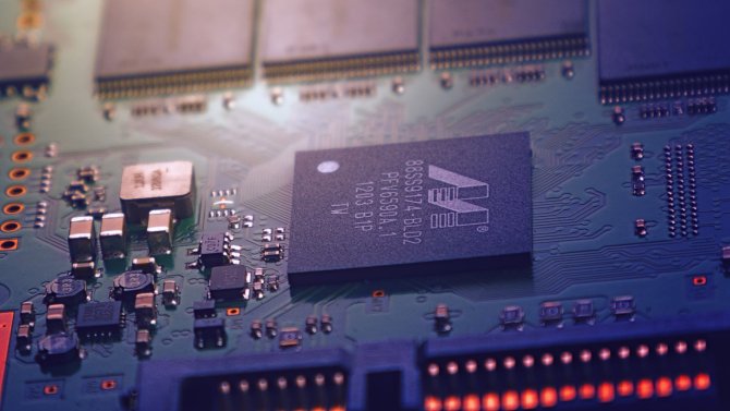
72 Qubit Quantum Computing Chip

The purpose of this gate-based superconducting system is to provide a testbed for research into system error rates and scalability of their qubit technology, as well as applications in quantum simulation, optimization, and machine learning. Qubits (the quantum version of traditional bits) are very unstable and can be adversely affected by noise, and most of these systems can only hold a state for less than 100 microseconds. Google believes that quantum supremacy can be “comfortably demonstrated” with 49 qubits and a two-qubit error below 0.5 percent. Previous quantum systems by Google have given two-qubit errors of 0.6 percent, which in theory sounds like an extremely small difference, but in the world of quantum computing remains significant.

However, each Bristlecone chip features 72 qubits, which may help mitigate some of this error, but as Google says, quantum computing isn’t just about qubits. Until now, the most advanced quantum chip, built by IBM, had 50 qubits.  “Operating a device such as Bristlecone at low system error requires harmony between a full stack of technology ranging from software and control electronics to the processor itself,” the team writes in a blog post. “Getting this right requires careful systems engineering over several iterations.”

(via Google Research Blog, Engadget, Forbes)


ARM’s Machine Learning Processors

ARM’s latest mobile processors are tuned to crunch machine-learning algorithms as efficiently as possible. ARM announced a few days ago that it has created its first dedicated machine-learning chips, which are meant for use in mobile and smart-home devices. The company says it’s sharing the plans with its hardware partners, including smartphone chipmaker Qualcomm, and expects to see devices packing the hardware by early 2019.

Currently, small and portable devices lack the power to run AI algorithms, so they enlist the help of big servers in the cloud. But enabling mobile devices to run their own AI software is attractive. It can speed things up, cutting the lag inherent in sending information back and forth. It will allow hardware to run offline. And it pleases privacy advocates, who are comforted by the idea of data remaining on the device.

ai_arm.jpg

Jem Davies, the lead of Machine Learning group at ARM, said, “We analyze compute workloads, work out which bits are taking the time and the power, and look to see if we can improve on our existing processors.”  The new chips use less power than the company’s other designs to perform the kinds of linear-algebra calculations that underpin modern artificial intelligence. They’re also better at moving data in and out of memory.

Artificial Synapse could make Brain-On-A-Chip Hardware a Reality

Let’s start by understanding what does the title mean! This is a part of Neuromorphic Engineering aka Neuromorphic Computing, describing the use of very-large-scale integration (VLSI) systems containing electronic analog circuits to mimic neuro-biological architectures present in the nervous system. Microprocessors configured more like brains than traditional chips could soon make computers far more astute about what’s going on around them.

neuromorphic.jpg

Neuromorphic computer chips are designed to work like the human brain. Instead of being controlled by binary, on-or-off signals like most current chips, neuromorphic chips weight their outputs, mimicking the way different neurons fire at different strengths through their synapses. In this way, small neuromorphic chips could, like the brain, efficiently process millions of streams of parallel computations that are currently only possible with large banks of supercomputers. But one significant hangup on the way to such portable artificial intelligence has been the neural synapse, which has been particularly tricky to reproduce in hardware.

Now engineers at MIT have designed an artificial synapse in such a way that they can precisely control the strength of an electric current flowing across it, similar to the way ions flow between neurons. The team has built a small chip with artificial synapses, made from silicon germanium. In simulations, the researchers found that the chip and its synapses could be used to recognize samples of handwriting, with 95 percent accuracy. The design, published last month in the journal Nature Materials, is a major step towards building portable, low-power neuromorphic chips for use in pattern recognition and other learning tasks.

Most neuromorphic chip designs attempt to emulate the synaptic connection between neurons using two conductive layers separated by a “switching medium,” or synapse-like space. When a voltage is applied, ions should move in the switching medium to create conductive filaments, similarly to how the “weight” of a synapse changes.

The research was led by Jeehwan Kim, the Class of 1947 Career Development Assistant Professor in the departments of Mechanical Engineering and Materials Science and Engineering, and a principal investigator in MIT’s Research Laboratory of Electronics and Microsystems Technology Laboratories.

In conclusion, Artificial neural networks are already loosely modeled on the brain. The combination of neural nets and neuromorphic chips could let AI systems be packed into smaller devices and run a lot more efficiently.


(via ScienceDaily, MitTechReview, Wiki)

Quantum Network

We all know the hype that’s currently running around Quantum Computer, their working and a plethora of discoveries happening in Quantum Computing. Recommended: Quantum ComputingQuantum Computer Memories.

Recently, there has been news about a Quantum Network or rather, Quantum Internet. So what’s Quantum Network? Quantum networks form an important element of quantum computing and quantum communication systems. In general, quantum networks allow for the transmission of quantum information (quantum bits, also called qubits), between physically separated quantum processors. A quantum processor is a small quantum computer being able to perform quantum logic gates on a certain number of qubits.

Quantum-TopArt-603192399.jpg

Being able to send qubits from one quantum processor to another allows them to be connected to form a quantum computing cluster. This is often referred to as networked quantum computing or distributed quantum computing. Here, several less powerful quantum processors are connected together by a quantum network to form one much more powerful quantum computer. This is analogous to connecting several classical computers to form a computer cluster in classical computing. Networked quantum computing offers a path towards scalability for quantum computers since more and more quantum processors can naturally be added over time to increase the overall quantum computing capabilities. In networked quantum computing, the individual quantum processors are typically separated only by short distances.

Going back a year, Chinese physicists launched the world’s first quantum satellite. Unlike the dishes that deliver your Television shows, this 1,400-pound behemoth doesn’t beam radio waves. Instead, the physicists designed it to send and receive bits of information encoded in delicate photons of infrared light. It’s a test of a budding technology known as quantum communications, which experts say could be far more secure than any existing info relay system. If quantum communications were like mailing a letter, entangled photons are kind of like the envelope: They carry the message and keep it secure. Jian-Wei Pan of the University of Science and Technology of China, who leads the research on the satellite, has said that he wants to launch more quantum satellites in the next five years.

The basic structure of a quantum network and more generally a quantum internet is analogous to classical networks. First, we have end nodes on which applications can ultimately be run. These end nodes are quantum processors of at least one qubit. Some applications of a quantum internet require quantum processors of several qubits as well as a quantum memory at the end nodes.

Second, to transport qubits from one node to another, we need communication lines. For the purpose of quantum communication, standard telecom fibers can be used. For networked quantum computing, in which quantum processors are linked at short distances, one typically employs different wavelength depending on the exact hardware platform of the quantum processor.

Third, to make maximum use of communication infrastructure, one requires optical switches capable of delivering qubits to the intended quantum processor. These switches need to preserve quantum coherence, which makes them more challenging to realize than standard optical switches.

Finally, to transport qubits over long distances one requires a quantum repeater. Since qubits cannot be copied, classical signal amplification is not possible and a quantum repeater works in a fundamentally different way than a classical repeater.

The quantum internet could also be useful for potential quantum computing schemes, says Fu. Companies like Google and IBM are developing quantum computers to execute specific algorithms faster than any existing computer. Instead of selling people personal quantum computers, they’ve proposed putting their quantum computer in the cloud, where users would log into the quantum computer via the internet. While running their computations, they might want to transmit quantum-encrypted information between their personal computer and the cloud-based quantum computer. “Users might not want to send their information classically, where it could eavesdrop,” Fu says. But still, this technology is almost 13 years away and surely we will witness a lot more discoveries in the coming years.

(source : MitTechReview, Wikipedia, Wired)


MIT’s new prototype ‘3D’ Chip

Daily a plethora of data is being generated and the computing power to process this data into useful information is stalling. One of the fundamental problems being faced is the processor-memory bottleneck or the performance gap. Various methods such as caches and different software techniques have been used to eliminate this problem. But there’s another way which is, building the CPU directly into a 3D memory structure, connect them directly without any kind of motherboard traces, and compute from within the RAM itself.

3d.jpeg


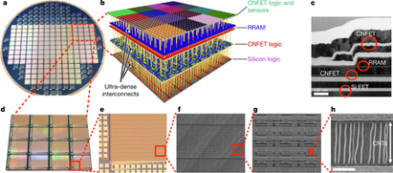
A prototype chip built by researchers at Stanford and MIT can solve the problem by sandwiching the memory, processor and even sensors all into one unit. While current chips are made of silicon

.

rram.jpg

The researchers have developed a new 3D chip fabrication method that uses carbon nanotubes and resistive random-access memory (RRAM) cells together to create a combined nanoelectronic processor design that supports complex, 3D architecture – where traditional silicon-based chip fabrication works with 2D structures only. The team claims this makes for “the most complex nanoelectronic system ever made with emerging nanotechnologies,” creating a 3D computer architecture. Using carbon makes the whole thing possible since higher temperatures required to make a silicon CPU would damage the sensitive RRAM cells.

The 3D design is possible because these carbon nanotube circuits and RRAM memory components can be made using temperatures below 200 degrees Celsius, which is far, far less than the 1,000 degree temps needed to fabricate today’s 2D silicon transistors. Lower temperatures mean you can build an upper layer on top of another without damaging the one or ones below.

One expert cited by MIT said that this could be the answer to continuing the exponential scaling of computer power in keeping with Moore’s Law, as traditional chip methods start to run up against physical limits. It’s still in its initial phases and it would take many years till we see the actual implementation of these chips in real life.

Intel Core i9

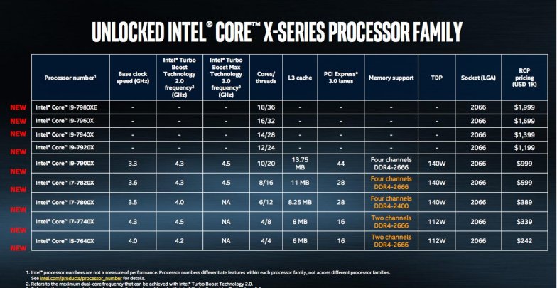
Intel recently announced a new family of processors for enthusiasts, the Core X-series, and it’s anchored by the company’s first 18-core CPU, the i9-7980XE.


Intel+Core+i9+x+series.jpg

Priced at $1,999, the 7980XE is clearly not a chip you’ll see in an average desktop. Instead, it’s more of a statement from Intel. It beats out AMD’s 16-core Threadripper CPU, which was slated to be that company’s most powerful consumer processor for 2017. And it gives Intel yet another way to satisfy the demands of power-hungry users who might want to do things like play games in 4K while broadcasting them in HD over Twitch. And, as if its massive core count wasn’t enough, the i9-7980XE is also the first Intel consumer chip that packs in over a teraflop’s worth of computing power.


inteli9.jpg


If 18 cores are overkill for you, Intel also has other Core i9 Extreme Edition chips in 10-, 12-, 14- and 16-core variants. Perhaps the best news for hardware geeks: The 10 Core i9-7900X will retail for $999, a significant discount from last year’s version.

All of the i9 chips feature base clock speeds of 3.3GHz, reaching up to 4.3GHz dual-core speeds with Turbo Boost 2.0 and 4.5GHz with Turbo Boost 3.0 a new version of Turbo Boost which Intel has upgraded. The company points out that while the additional cores on the Core X models will improve multitasking performance, the addition of technologies like Turbo Boost Max 3.0 ensures that each core is also able to achieve improved performance. (Intel claims that the Core X series reaches 10 percent faster multithread performance over the previous generation and 15 percent faster single thread.)


(via Engadget, The Verge)


Google’s and Nvidia’s AI Chips

Google

Google will soon launch a cloud computing service that provides exclusive access to a new kind of artificial intelligence chip designed by its own engineers. CEO Sundar Pichai revealed the new chip and service this morning in Silicon Valley during his keynote at Google I/O, the company’s annual developer conference.

GoogleChip4.jpg

This new processor is a unique creation designed to both train and execute deep neural networks—machine learning systems behind the rapid evolution of everything from image and speech recognition to automated translation to robotics. Google says it will not sell the chip directly to others. Instead, through its new cloud service, set to arrive sometime before the end of the year, any business or developer can build and operate software via the internet that taps into hundreds and perhaps thousands of these processors, all packed into Google data centers.

According to Dean, Google’s new “TPU device,” which spans four chips, can handle 180 trillion floating point operations per second, or 180 teraflops, and the company uses a new form of computer networking to connect several of these chips together, creating a “TPU pod” that provides about 11,500 teraflops of computing power. In the past, Dean said, the company’s machine translation model took about a day to train on 32 state-of-the-art CPU boards. Now, it can train in about six hours using only a portion of a pod.

Nvidia

Nvidia has released a new state-of-the-art chip that pushes the limits of machine learning, the Tesla P100 GPU. It can perform deep learning neural network tasks 12 times faster than the company’s previous top-end system (The TitanX). The P100 was a huge commitment for Nvidia, costing over $2 billion in research and development, and it sports a whopping 150 billion transistors on a single chip, making the P100 the world’s largest chip, Nvidia claims. In addition to machine learning, the P100 will work for all sorts of high-performance computing tasks — Nvidia just wants you to know it’s really good at machine learning.

dgx.png

To top off the P100’s introduction, Nvidia has packed eight of them into a crazy-powerful $129,000 supercomputer called the DGX-1. This show-horse of a machine comes ready to run, with deep-learning software preinstalled. It’s shipping first to AI researchers at MIT, Stanford, UC Berkeley, and others in June. On stage, Huang called the DGX-1 “one beast of a machine.”

The competition between these upcoming AI chips and Nvidia all points to an emerging need for simply more processing power in deep learning computing. A few years ago, GPUs took off because they cut the training time for a deep learning network from months to days. Deep learning, which had been around since at least the 1950s, suddenly had real potential with GPU power behind it. But as more companies try to integrate deep learning into their products and services, they’re only going to need faster and faster chips.


(via Wired, Forbes, Nvidia, The Verge)


Artificial Intelligence ready ARM CPUs (DynamIQ)

ARM processors are ubiquitous and many of the tech gadgets we used are powered by them, furthermore, the company is showing off its plans for the future with DynamIQ. Aimed squarely at pushing the artificial intelligence and machine learning systems we’re expecting to see in cars, phones, gaming consoles and everything else, it’s what the company claims is an evolution on the existing “big.Little” technology.

arm.jpg

Here’s a high-level look at some of the new features, capabilities and benefits DynamIQ will bring to new Cortex-A processors later this year:

  • New dedicated processor instructions for ML and AI: Cortex-A processors designed for DynamIQ technology can be optimized to deliver up to a 50x boost in AI performance over the next 3-5 years relative to Cortex-A73-based systems today and up to 10x faster response between CPU and specialized accelerator hardware on the SoC that can unleash substantially better-combined performance.

arm-dynamiq2.jpg

  • Increased multi-core flexibility: SoC designers can scale up to eight cores in a single cluster and each core can have different performance and power characteristics. These advanced capabilities enable faster responsiveness to ML and AI applications. A redesigned memory subsystem enables both faster data access and enhance power management
  • More performance within restricted thermal budgets: Efficient and much faster switching of software tasks to match the right-sized processor for optimal performance and power is further enhanced through independent frequency control of individual processors
  • Safer autonomous systems: DynamIQ brings greater levels of responsiveness for ADAS solution and increased safety capabilities which will enable partners to build ASIL-D compliant systems for safe operation under failure conditions.


(source: ARM community, Engadget)

Quantum computer memories of higher dimensions than a qubit

A quantum computer memory of higher dimensions has been created by the scientists from the Institute of Physics and Technology of the Russian Academy of Sciences and MIPT by letting two electrons loose in a system of quantum dots. In their study published in Scientific Reports, the researchers demonstrate for the first time how quantum walks of several electrons can help for implementation of quantum computation.

For more information: Quantum Computing

walking-electrons

Abstraction – Walking Electrons

“By studying the system with two electrons, we solved the problems faced in the general case of two identical interacting particles. This paves the way toward compact high-level quantum structures,” says Leonid Fedichkin, associate professor at MIPT’s Department of Theoretical Physics.

In a matter of hours, a quantum computer will be able to hack into the most popular cryptosystem used by web browsers. As far as more benevolent applications are concerned, a quantum computer would be capable of molecular modeling that accounts for all interactions between the particles involved. This, in turn, would enable the development of highly efficient solar cells and new drugs.

As it turns out, the unstable nature of the connection between qubits remains the major obstacle preventing the use of quantum walks of particles for quantum computation. Unlike their classical analogs, quantum structures are extremely sensitive to external noise. To prevent a system of several qubits from losing the information stored in it, liquid nitrogen (or helium) needs to be used for cooling. A research team led by Prof. Fedichkin demonstrated that a qubit could be physically implemented as a particle “taking a quantum walk” between two extremely small semiconductors known as quantum dots, which are connected by a “quantum tunnel.”

The Quantum dots are like potential wells to an electron, therefore, the position of an electron can be used to encode the basis of two states of the qubits 0 or 1.

elec.jpg

The blue and purple dots in the diagrams are the states of the two connected qudits (qutrits and ququarts are shown in (a) and (b) respectively). Each cell in the square diagrams on the right side of each figure (a-d) represents the position of one electron (i = 0, 1, 2, … along the horizontal axis) versus the position of the other electron (j = 0, 1, 2, … along the vertical axis). The cells color-code the probability of finding the two electrons in the corresponding dots with numbers i and j when a measurement of the system is made. Warmer colors denote higher probabilities. Credit: MIPT

If an entangled state is created between several qubits, their individual states can no longer be described separately from one another, and any valid description must refer to the state of the whole system. This means that a system of three qubits has a total of eight basis states and is in a superposition of them: A|000⟩+B|001⟩+C|010⟩+D|100⟩+E|011⟩+F|101⟩+G|110⟩+H|111⟩. By influencing the system, one inevitably affects all of the eight coefficients, whereas influencing a system of regular bits only affects their individual states. By implication, n bits can store n variables, while n qubits can store 2n variables. Qudits offer an even greater advantage since n four-level qudits (aka ququarts) can encode 4n, or 2n×2n variables. To put this into perspective, 10 ququarts store approximately 100,000 times more information than 10 bits. With greater values of n, the zeros in this number start to pile up very quickly.

In this study, Alexey Melnikov and Leonid Fedichkin obtain a system of two qudits implemented as two entangled electrons quantum-walking around the so-called cycle graph. The entanglement of the two electrons is caused by the mutual electrostatic repulsion experienced by like charges. Number of qudits can be created by connecting quantum dots in a pattern of winding paths and have more wandering electrons. The quantum walks approach to quantum computation is convenient because it is based on a natural process.

So far, scientists have been unable to connect a sufficient number of qubits for the development of a quantum computer. The work of the Russian researchers brings computer science one step closer to a future when quantum computations are commonplace.

(Source: Moscow Institute of Physics and Technology, 3Tags.)

World’s First Fully Programmable and Reconfigurable Quantum Computer Module

A team of researchers, led by Professor Christopher Monroe from Joint Quantum Institute (JQI) at the University of Maryland Physics , has introduced the first fully programmable and reconfigurable quantum computer module in a paper published as the cover article in the August 4 issue of the journal Nature.

For more Info: Read Quantum Computing.


pions.jpg

Photo of an ion trap.


The new device, dubbed a module because of its potential to connect with copies of itself is made of five individual ions, charged atoms — trapped in a magnetic field, whose strength is manipulated in such a way that the ions are arranged in a line. A computer program dedicated to solving a particular problem—on five quantum bits, or qubits—the fundamental unit of information in a quantum computer. Quantum computers promise speedy solutions to some difficult problems, but building large-scale, general-purpose quantum devices is a problem fraught with technical challenges.

“For any computer to be useful, the user should not be required to know what’s inside,” said Monroe, who is also a UMD Distinguished University Professor, the Bice Zorn Professor of Physics, and a fellow of the Joint Quantum Institute and the Joint Center for Quantum Information and Computer Science. “Very few people care what their iPhone is actually doing at the physical level. Our experiment brings high-quality quantum bits up to a higher level of functionality by allowing them to be programmed and reconfigured in software.”

The reconfigurability of the laser beams is a key advantage, Debnath says. “By reducing an algorithm into a series of laser pulses that push on the appropriate ions, we can reconfigure the wiring between these qubits from the outside,” he said. “It becomes a software problem, and no other quantum computing architecture has this flexibility.”

To test the module, the team ran three different quantum algorithms, including a demonstration of a Quantum Fourier Transform (QFT), which finds how often a given mathematical function repeats. It is a key piece in Shor’s quantum factoring algorithm, which would break some of the most widely-used security standards on the internet if run on a big enough quantum computer.

Two of the algorithms ran successfully more than 90 percent of the time, while the QFT topped out at a 70 percent success rate. The team says that this is due to residual errors in the pulse-shaped gates as well as systematic errors that accumulate over the course of the computation, neither of which appear fundamentally insurmountable. They note that the QFT algorithm requires all possible two-qubit gates and should be among the most complicated quantum calculations.

The team believes that eventually more qubits—perhaps as many as 100—could be added to their quantum computer module. It is also possible to link separate modules together, either by physically moving the ions or by using photons to carry information between them.


(via Science Daily, IBT)